
Tiny USB 3.0 Hub
Open source, tiny (~penny-sized) USB 3.2 Gen 1x1 hub for distributed sensing applications.
Documentation: https://docs.google.com/document/d/1O4f5b7Dc3Jj556MIkbM53eZpJiqbKlDK-BqDew--iZo/edit?usp=sharing
Description
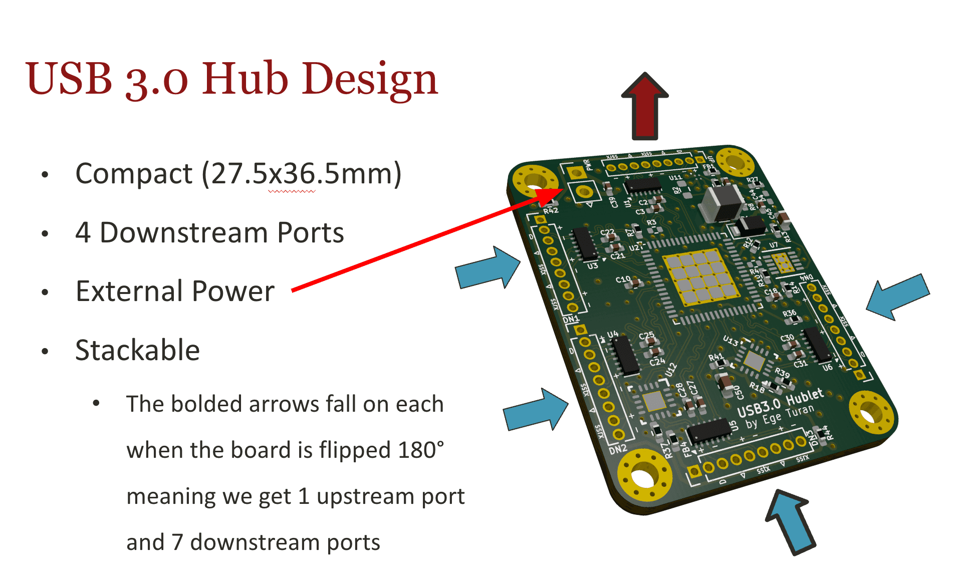
A tiny (penny-sized) 4-port USB 3.2 Gen 1x1 hub designed for distributed sensing networks.
Supports USB 3.0 and USB 2.0, with 5 Gbps SuperSpeed bandwidth using the TI TUSB8041.
Features individual port power control, ESD protection, and can operate as bus-powered or with external power.
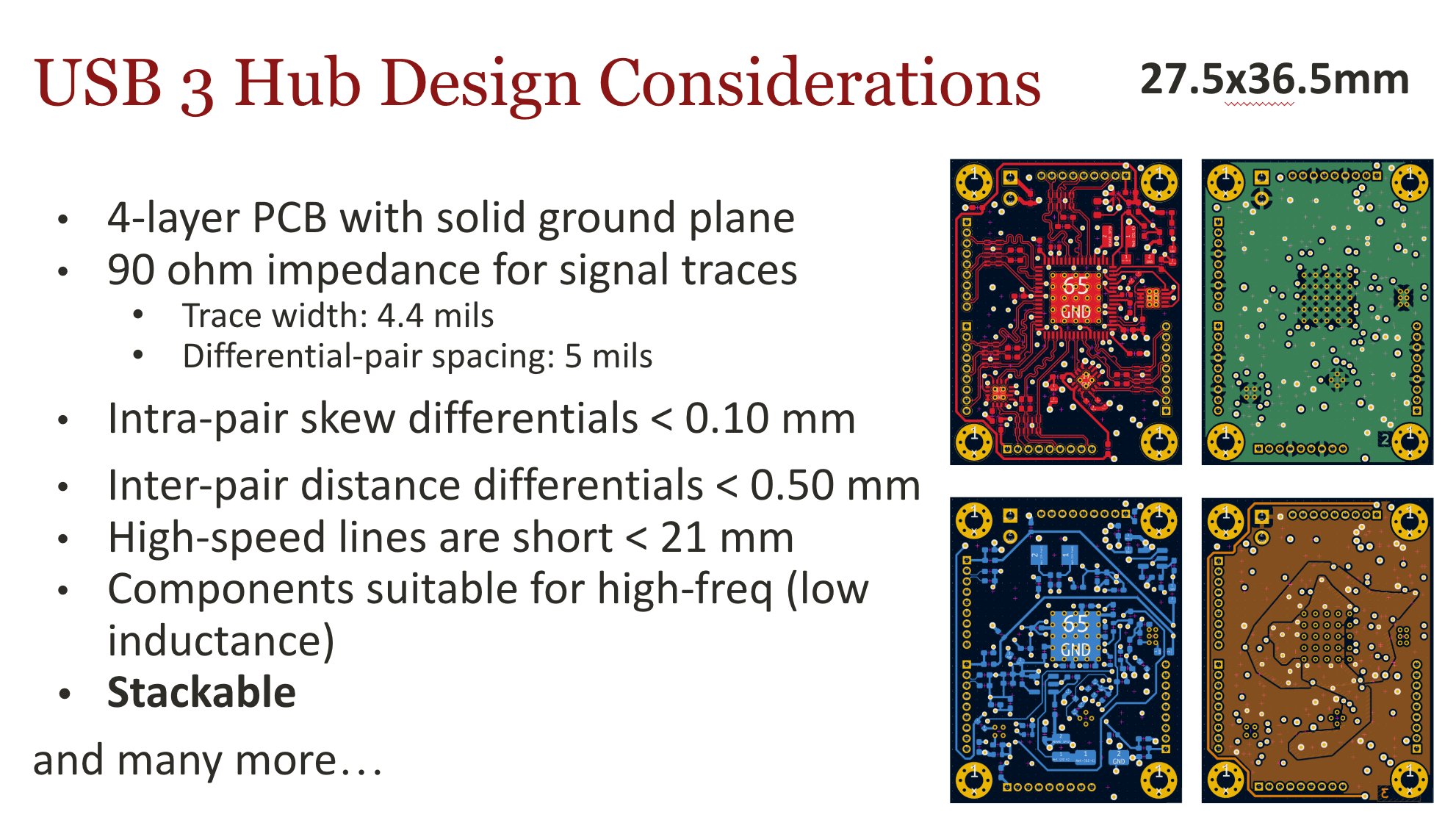
Built on a 4-layer PCB (27.5 × 36.5 mm) optimized for signal integrity, heat dissipation, and high-speed differential pair routing.
Designed for integration into size- and weight-constrained systems such as whole-body sensing networks on free-space vine robots.
Fully open-source, with schematics, PCB, and test scripts available.
Learning Outcomes
1. Technical Skills & Knowledge
High-speed PCB design: USB 3.0 impedance matching, intra-/inter-pair skew, signal integrity
Development using TI TUSB8041 and debugging using the official TUSB8041EVM dev board
Power distribution, current handling, and protection circuitry (OC, ESD)
Thermal analysis, voltage rail diagnostics, and bring-up troubleshooting
Prototyping and testing with multiple USB cameras and scripted tools (e.g., OpenCV)
2. General Project/Practical Skills
Systems Engineering: High-frequency electronics design, testing, and iteration under tight space constraints
Failure analysis and debugging: Hardware bring-up with thermal and electrical diagnostics
Documentation and collaboration: Detailed technical documentation, lab notes, and presentation of results
Open-source hardware development: BOM optimization, manufacturability for small-scale assembly (e.g., JLCPCB)
Open source, tiny (~penny-sized) USB 3.2 Gen 1x1 hub for distributed sensing applications
Open source, tiny USB 3.2 Gen 1x1 hub designed for distributed sensing applications, featuring 4 ports, individual power control, and ESD protection. It supports USB 3.0 with 5 Gbps bandwidth and is optimized for integration into compact systems. Key learning outcomes include high-speed PCB design, systems engineering, failure analysis, and open-source hardware development.